

This section provides a detailed overview of the XBee module’s pinout for each layout, explaining the function and purpose of each pin to help you correctly integrate the device into your design.
Through-hole (TH) module
The following drawing shows the through-hole pin locations.
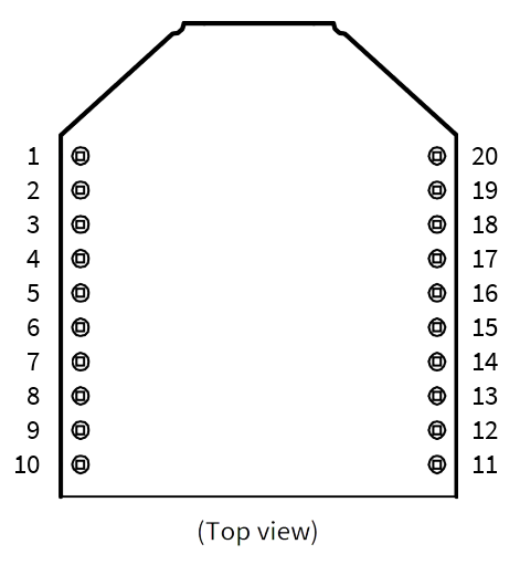
The following table shows the pin signals and their descriptions for the XBee for Wi-SUN through-hole device:
| Pin# | Name | Direction | Default state | Description |
|---|---|---|---|---|
1 |
VCC |
- |
- |
Power supply. |
2 |
DOUT/DIO13 |
Both |
Output |
UART data out/GPIO. |
3 |
DIN/CONFIG/DIO14 |
Both |
Intput |
UART data in/GPIO. |
4 |
DIO12/SPI_MISO |
Both |
- |
GPIO/SPI data out. |
5 |
RESET |
Input |
- |
Device reset. |
6 |
RSSI_PWM/DIO10 |
Both |
Output |
RX signal strength Indicator/GPIO. |
7 |
PWM1/DIO11/I2C_SDA |
Both |
Disabled |
Pulse width modulator/GPIO/I2C_SDA. |
8 |
[reserved] |
- |
Disabled |
Do not connect. |
9 |
DTR/SLEEP_RQ/DIO8 |
Both |
Input |
Pin sleep control Line/GPIO. |
10 |
GND |
- |
- |
Ground. |
11 |
DIO4/SPI_MOSI |
Both |
Disabled |
GPIO/Serial peripheral interface data in. |
12 |
CTS/DIO7 |
Both |
Output |
Clear to send flow control/GPIO. |
13 |
ON/SLEEP/DIO9 |
Both |
Output |
Device status indicator/GPIO. |
14 |
[reserved] |
- |
Disabled |
Do not connect or connect to Ground. |
15 |
ASSOCIATE/DIO5 |
Both |
Output |
Associate Indicator/GPIO. |
16 |
RTS/DIO6 |
Both |
Input |
Request to send flow control/GPIO. |
17 |
AD3/DIO3/SPI_SSEL |
Both |
Disabled |
Analog input/GPIO/SPI not select. |
18 |
AD2/DIO2/SPI_CLK |
Both |
Disabled |
Analog input/GPIO/SPI clock. |
19 |
AD1/DIO1/SPI_ATTN/I2C_SCL |
Both |
Disabled |
Analog input/GPIO/SPI attention/I2C_SCL. |
20 |
AD0/DIO0 |
Both |
Input |
Analog input/GPIO/Commissioning button. |
Signal direction is specified with respect to the device. |
||||
Micro-mount (MMT) module
The following drawing shows the micro-mount pin locations.
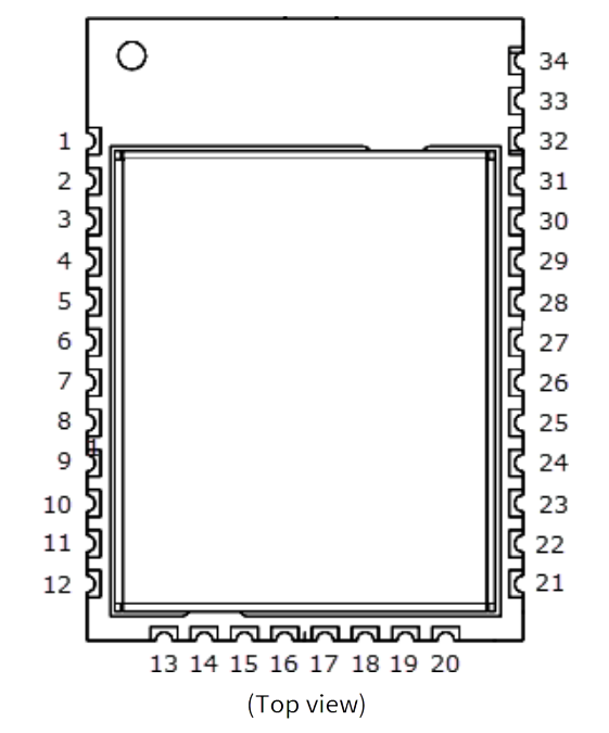
The following table shows the pin signals and their descriptions for the XBee for Wi-SUN micro-mount device:
| Pin# | Name | Direction | Default state | Description |
|---|---|---|---|---|
1 |
GND |
- |
- |
Ground. |
2 |
VCC |
- |
- |
Power supply. |
3 |
DOUT/DIO13 |
Both |
Output |
UART data out/GPIO. |
4 |
DIN/CONFIG/DIO14 |
Both |
Input |
UART data in/GPIO. |
5 |
DIO12 |
Both |
- |
GPIO. |
6 |
RESET |
Input |
- |
Device reset. |
7 |
RSSI_PWM/DIO10 |
Both |
Output |
RX signal strength Indicator/GPIO. |
8 |
PWM1/DIO11/I2C_SDA |
Both |
Disabled |
Pulse width modulator/GPIO/I2C_SDA. |
9 |
DTR/SLEEP_RQ/DIO8 |
Both |
Input |
Pin sleep control Line/GPIO. |
10 |
GND |
- |
- |
Ground. |
11 |
SPI_ATTN/BOOTMODE/DIO19 |
Output |
Output |
Serial peripheral interface attention. |
12 |
GND |
- |
- |
Ground. |
13 |
SPI_CLK/DIO18 |
Input |
Input |
Serial peripheral interface clock/GPIO. |
14 |
SPI_SSEL/DIO17 |
Input |
Input |
Serial peripheral interface not select/GPIO. |
15 |
SPI_MOSI/DIO16 |
Input |
Input |
Serial peripheral interface data in/GPIO. |
16 |
SPI_MISO/DIO15 |
Output |
Output |
Serial peripheral interface data out/GPIO. |
17 |
[reserved] |
- |
Disabled |
Do not connect. |
18 |
[reserved] |
- |
Disabled |
Do not connect. |
19 |
[reserved] |
- |
Disabled |
Do not connect. |
20 |
[reserved] |
- |
Disabled |
Do not connect. |
21 |
GND |
- |
- |
Ground. |
22 |
[reserved] |
- |
Disabled |
Do not connect. |
23 |
DIO4 |
Both |
Disabled |
GPIO. |
24 |
CTS/DIO7 |
Both |
Output |
Clear to send flow control/GPIO. |
25 |
ON/SLEEP/DIO9 |
Both |
Output |
Device status indicator/GPIO. |
26 |
ASSOCIATE/DIO5 |
Both |
Output |
Associate Indicator/GPIO. |
27 |
RTS/DIO6 |
Both |
Input |
Request to send flow control/GPIO. |
28 |
AD3/DIO3 |
Both |
Disabled |
Analog input/GPIO. |
29 |
AD2/DIO2 |
Both |
Disabled |
Analog input/GPIO. |
30 |
AD1/DIO1/I2C_SCL |
Both |
Disabled |
Analog input/GPIO/I2C_SCL. |
31 |
AD0/DIO0 |
Both |
Input |
Analog input/GPIO/Commissioning button. |
32 |
GND |
- |
- |
Ground. |
33 |
RF |
Both |
- |
RF I/O for RF pad variant. |
34 |
GND |
- |
- |
Ground. |
Signal direction is specified with respect to the device. |
||||
Surface-mount (SMT) module
The following drawing shows the surface-mount pin locations.
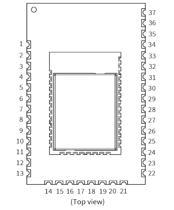
The following table shows the pin signals and their descriptions for the XBee for Wi-SUN surface-mount device:
| Pin# | Name | Direction | Default state | Description |
|---|---|---|---|---|
1 |
GND |
- |
- |
Ground. |
2 |
VCC |
- |
- |
Power supply. |
3 |
DOUT/DIO13 |
Both |
Output |
UART data out/GPIO. |
4 |
DIN/CONFIG/DIO14 |
Both |
Input |
UART data in/GPIO. |
5 |
DIO12 |
Both |
- |
GPIO. |
6 |
RESET |
Input |
- |
Device reset. |
7 |
RSSI_PWM/DIO10 |
Both |
Output |
RX signal strength Indicator/GPIO. |
8 |
PWM1/DIO11/I2C_SDA |
Both |
Disabled |
Pulse width modulator/GPIO/I2C_SDA. |
9 |
[reserved] |
- |
Disabled |
Do not connect. |
10 |
DTR/SLEEP_RQ/DIO8 |
Both |
Input |
Pin sleep control Line/GPIO. |
11 |
GND |
- |
- |
Ground. |
12 |
SPI_ATTN/BOOTMODE/DIO19 |
Output |
Output |
Serial peripheral interface attention. |
13 |
GND |
- |
- |
Ground. |
14 |
SPI_CLK/DIO18 |
Input |
Input |
Serial peripheral interface clock/GPIO. |
15 |
SPI_SSEL/DIO17 |
Input |
Input |
Serial peripheral interface not select/GPIO. |
16 |
SPI_MOSI/DIO16 |
Input |
Input |
Serial peripheral interface data in/GPIO. |
17 |
SPI_MISO/DIO15 |
Output |
Output |
Serial peripheral interface data out/GPIO. |
18 |
[reserved] |
- |
Disabled |
Do not connect. |
19 |
[reserved] |
- |
Disabled |
Do not connect. |
20 |
[reserved] |
- |
Disabled |
Do not connect. |
21 |
[reserved] |
- |
Disabled |
Do not connect. |
22 |
GND |
- |
- |
Ground. |
23 |
[reserved] |
- |
Disabled |
Do not connect. |
24 |
DIO4 |
Both |
Disabled |
GPIO. |
25 |
CTS/DIO7 |
Both |
Output |
Clear to send flow control/GPIO. |
26 |
ON/SLEEP/DIO9 |
Both |
Output |
Device status indicator/GPIO. |
27 |
[reserved] |
- |
Disabled |
Do not connect or connect to Ground. |
28 |
ASSOCIATE/DIO5 |
Both |
Output |
Associate Indicator/GPIO. |
29 |
RTS/DIO6 |
Both |
Input |
Request to send flow control/GPIO. |
30 |
AD3/DIO3 |
Both |
Disabled |
Analog input/GPIO. |
31 |
AD2/DIO2 |
Both |
Disabled |
Analog input/GPIO. |
32 |
AD1/DIO1/I2C_SCL |
Both |
Disabled |
Analog input/GPIO/I2C_SCL. |
33 |
AD0/DIO0 |
Both |
Input |
Analog input/GPIO/Commissioning button. |
34 |
[reserved] |
- |
Disabled |
Do not connect. |
35 |
GND |
- |
- |
Ground. |
36 |
RF |
Both |
- |
RF I/O for RF pad variant. |
37 |
[reserved] |
- |
Disabled |
Do not connect. |
Signal direction is specified with respect to the device. |
||||