

An Analog-to-Digital Converter (ADC) is a device that translates an analog voltage to a digital value that a microprocessor can understand.
The STMicroelectronics system-on-module has two ADC controllers, each with up to 19 channels. The ADC controllers are 12-bit successive approximation analog-to-digital converters.
Available ADC pins
On the ConnectCore MP13:
-
A number of ADC channels are available at castellated and LGA pads, multiplexed with other functions. Check the Hardware reference manuals for information about pads and ADC channels.
On the ConnectCore MP13 Development Kit:
-
GPIOA 5 (ADC1 channel 2) is accessible on
MIKROBUS_PWMline, connector J31
Kernel configuration
You can manage the STM32MP13 ADC drivers support through the following kernel configuration options:
-
STM32 ADC core driver (
CONFIG_STM32_ADC_CORE) -
STM32 ADC driver (
CONFIG_STM32_ADC)
These options are enabled as built-in on the default ConnectCore MP13 kernel configuration file.
Kernel driver
The ADC drivers are located at:
| File | Description |
|---|---|
STM32MP13 ADC core driver |
|
STM32MP13 ADC driver |
Device tree bindings and customization
The STM32MP13 ADC device tree binding is documented at
Documentation/devicetree/bindings/iio/adc/st,stm32-adc.yaml.
The device tree must contain entries for:
-
The ADC interfaces
-
The enabled channels
-
The IOMUX (for ADC channels on non-dedicated pads)
STM32MP13 ADC interfaces and channels
The STM32MP13 device tree defines:
-
The two ADC interfaces as child nodes of the ADC core
-
The channels of each interface as child nodes inside each ADC interface
adc_1: adc@48003000 {
	compatible = "st,stm32mp13-adc-core";
	[...]
	status = "disabled";

	adc1: adc@0 {
		compatible = "st,stm32mp13-adc";
		[...]
		status = "disabled";

		channel@18 {
			reg = <18>;
			label = "vrefint";
		};
	};
};

adc_2: adc@48004000 {
	compatible = "st,stm32mp13-adc-core";
	[...]
	status = "disabled";

	adc2: adc@0 {
		compatible = "st,stm32mp13-adc";
		[...]
		status = "disabled";

		channel@13 {
			reg = <13>;
			label = "vrefint";
		};
		channel@14 {
			reg = <14>;
			label = "vddcore";
		};
		channel@16 {
			reg = <16>;
			label = "vddcpu";
		};
		channel@17 {
			reg = <17>;
			label = "vddq_ddr";
		};
	};
};
ConnectCore MP13 Development Kit ADC interfaces and channels
-
ADC1 channel 2 is enabled on GPIO
PA5.
&adc_1 {
	/* PA5 which is shared with MikroE PWM */
	pinctrl-names = "default";
	pinctrl-0 = <&ccmp13_adc1_pins>;
	/* External Vref (requires connecting external voltage to VREF+ pad) */
	vref-supply = <&external_vref>;
	/* Internal Vref (requires enabling VREFBUF in OP-TEE device tree) */
	//vref-supply = <&scmi_vrefbuf>;
	status = "okay";

	adc1: adc@0 {
		status = "okay";

		channel@2 {
			reg = <2>;
			label = "PA5"
			st,min-sample-time-nsecs = <5000>;
		};
	};
};

[...]

&pinctrl {
	ccmp13_adc1_pins: ccmp13_adc1-pins-0 {
		pins {
			pinmux = <STM32_PINMUX('A', 5, ANALOG)>; /* ADC1 in2 */
		};
	};
};
Select and configure an ADC channel
Follow these steps to configure ADC channels on your custom design:
-
Identify the pins you want configured as ADC on the Hardware reference manuals. Pins that are ADC-capable list an additional function like
ADCn_INPx, where n is the ADC interface and x the channel. -
Add a
channel@xas a subnode of the ADCn interface, and propertyreg = <x>;inside. -
Configure the IOMUX of the pads to operate as
ANALOGinputs.
For example, pad PA5 of the CPU has additional function ADC1_INP2.
This pad is available on the ConnectCore MP13 Development Kit mikroBUS™ socket connector.
&adc1 {
	status = "okay";

	channel@2 {
		reg = <2>;
		label = "PA5";
		st,min-sample-time-nsecs = <400>;
	};
};

&pinctrl {
	ccmp13_adc_pins: ccmp13_adc_pins-0 {
		pins {
			pinmux = <STM32_PINMUX('A', 5, ANALOG)>;
		};
	};
};
Voltage reference
The ADC block supports the following voltage references:
-
Internal VREFBUF regulator
-
External voltage reference (needs to be supplied through
VREF+pad).
Internal voltage reference (VREFBUF regulator)
VREFBUF is a STM32MP13 internal voltage regulator supplied via the scmi_vdd_adc regulator of the PMIC.
You can configure VREFBUF to supply one of the following voltages to output at the VREF+ pin:
-
2.5 V
-
2.048 V
-
1.8 V
-
1.65 V
On the ConnectCore MP13, the ADC voltage reference is configured to use an external voltage reference, and the internal VREFBUF is disabled.
To configure the ADC to use the VREFBUF regulator as voltage reference, make the following change to your Linux device tree:
diff --git a/arch/arm/boot/dts/ccmp133-dvk.dts b/arch/arm/boot/dts/ccmp133-dvk.dts
index 3ae234f75eab..a8f8cafca77b 100644
--- a/arch/arm/boot/dts/ccmp133-dvk.dts
+++ b/arch/arm/boot/dts/ccmp133-dvk.dts
@@ -138,10 +138,10 @@ &adc_1 {
        pinctrl-names = "default";
        pinctrl-0 = <&ccmp13_adc1_pins>;
        /* External Vref (requires connecting external voltage to VREF+ pad) */
-       vref-supply = <&external_vref>;
+       // vref-supply = <&external_vref>;
        /* Internal Vref (this outputs VREFBUF voltage at VREF+ pad) */
-       //vref-supply = <&scmi_vrefbuf>;
+       vref-supply = <&scmi_vrefbuf>;
        status = "okay";

        adc1: adc@0 {
Optionally, you can configure the regulator to your desired voltage (2.5 V by default):
/*
 * VREFBUF can be set to 2.5 V, 2.048 V, 1.8 V or 1.65 V which are
 * output at VREF+ pad.
 */
&scmi_vrefbuf {
	regulator-min-microvolt = <2500000>;
	regulator-max-microvolt = <2500000>;
};
If you plan to measure signals of less voltage, you can get more accurate results by changing the regulator-min-microvolt and regulator-max-microvolt properties to any of the other voltages.
|
External voltage reference
You can use an external voltage reference for the ADC. This external voltage reference must be between the limits:
-
Min: 1.62 V
-
Max: 3.3 V
To use an external voltage reference:
-
Add a fixed regulator node for the external regulator, with its voltage: For example:
/ { regulators { /* * External regulator for ADC. * This regulator DOES NOT exist on the DVK. It is only * a helper for testing the ADC channels. * To make use of it, you need to supply externally the * configured voltage to the VREF+ pad. * * NOTE: This is incompatible with using the internal VREFBUF * regulator, which outputs a voltage at VREF+ pad. */ external_vref: regulator@99 { reg = <99>; compatible = "regulator-fixed"; regulator-name = "external-vref"; regulator-min-microvolt = <3300000>; regulator-max-microvolt = <3300000>; }; }; }; -
Set the property
vref-supplyof the ADC node to use the external regulator:&adc_1 { vref-supply = <&external_vref>; }; -
If enabled, disable the internal
vrefbufregulator. See Internal voltage reference (VREFBUF regulator). -
Enable the VDDA regulator to remain on all the time. This prevents the analog block drain voltage out of your external voltage reference when the system is not using it.
&scmi_vdd_adc { regulator-always-on; }; -
Supply the external voltage at
VREF+pad.
Formula
The value read on the ADC inputs responds to the formula:
\$V = (V_(RAW) + V_(OFFSET)) * V_(SCALE)\$
where:
-
VRAW is the input voltage converted by the ADC.
-
VOFFSET is the ADC voltage offset.
-
VSCALE is the ADC voltage scale value. This is automatically calculated basing on the Voltage reference on your device tree.
Using the ADCs
The ADC drivers are designed as standard Industrial I/O (IIO) device drivers that can be accessed from the sysfs or from user applications.
If you are using the external voltage reference (default), you must supply an external voltage at VREF+.
See External voltage reference.
|
Sysfs access
When enabled, the ADC drivers create the corresponding device entries in the IIO sysfs directory (/sys/bus/iio/devices).
To determine which entry corresponds to which driver, read the name descriptors with:
# grep -H "" /sys/bus/iio/devices/iio\:device*/name
/sys/bus/iio/devices/iio:device0/48003000.adc:adc@0
In this example, device0 corresponds to ADC1.
The driver creates:
-
A file entry
in_voltage_offsetwith the voltage offset. -
A file entry
in_voltage_scalewith the voltage scale. -
A file entry
in_voltageX_rawfor each ADC channel, where X corresponds to the channel number.
Read the input value of a channel with:
# cat /sys/bus/iio/devices/iio\:device0/in_voltage2_raw
4030
# cat /sys/bus/iio/devices/iio\:device0/in_voltage_offset
0
# cat /sys/bus/iio/devices/iio\:device0/in_voltage_scale
0.805664062
The returned value in in_voltage2_raw is a decimal number with the result of the conversion.
In the example, and according to the Formula:
Sample application
An example application called apix-adc-example is included in the dey-examples-digiapix recipe (part of dey-examples package) of the meta-digi layer.
This application shows how to access the ADCs using Digi APIx library on the ConnectCore MP13 platform.
Go to GitHub to see the application instructions and source code.
See ADC API for more information about the ADC APIx.
Differential mode
In differential mode, the analog voltage to be converted for a channel is equal to the difference between the voltages at ADCn_INPx (positive input) and ADCn_INNx (negative input).
The converted raw value read from the ADC is calculated in the following way.
Configure differential mode
To enable differential mode, on your Linux device tree:
-
Select the ADC channel node that corresponds to the
ADCn_INPxfunctionality (positive input) -
Add to this node the property
diff-channels = <x y>, where:-
xis the channel number for theADCn_INPxfunctionality (positive input) -
yis-
the channel number for the
ADCn_INPyfunctionality that also multiplexesADCn_INNx(negative input), or -
any channel number if
ADCn_INNxis connected to VSSA internally
-
-
|
Refer to the chapter Pad signals and multiplexing of the https://www.digi.com/resources/documentation/digidocs/90002551/#reference/r_external-signals-multiplexing.htm Hardware Reference Manual to locate the pads that have the additional functionality Refer to ADC1 connectivity and ADC2 connectivity of the STMicroelectronics STM32MP13 Hardware Reference Manual, for information on internal connections of |
For instance, we locate ADC1_INP2 on pad PA5:
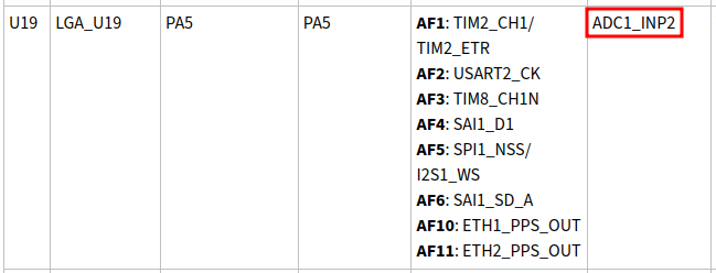
This is ADC1 channel 2 positive input. (x is 2.)
Now we need to locate ADC1 channel 2 negative input, that is ADC1_INN2.
We find this functionality on pad PF12
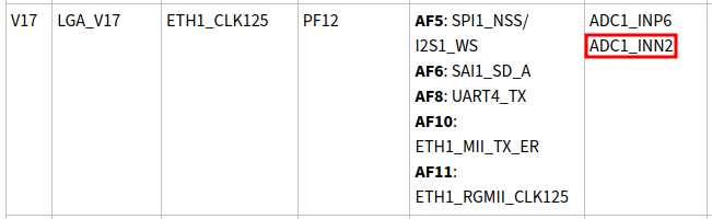
To find the y, we need to select the channel positive input that’s multiplexed on that same pad for ADC1.
This is ADC1_INP6. (y is 6.)
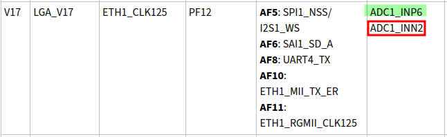
So, with a property diff-channels = <2 6>; we can measure the voltage difference (ADC1_INP2 - ADC1_INN2).
The device tree would look like this:
	adc1: adc@0 {
		status = "okay";

		channel@2 {
			reg = <2>;
			label = "INP2-INN2";
			diff-channels = <2 6>;
			st,min-sample-time-ns = <10000>;
		};
	};
This device tree excerpt is limited to the ADC.
If the used pads are not analog-dedicated, you also need to configure their pinctrl to ANALOG, and disable any conflicting interface that’s trying to make use of such pads for a different purpose.
|
Read the value of a differential channel
When configured in differential mode, the offset and scale values are different than those in normal mode.
Check the offset and scale values:
# cat /sys/bus/iio/devices/iio\:device0/in_voltage-voltage_offset
-2048
# cat /sys/bus/iio/devices/iio\:device0/in_voltage-voltage_scale
1.611328125
To read the value of the differential ADC channel:
# cat /sys/bus/iio/devices/iio\:device0/in_voltage2-voltage6_raw
2715
To calculate the voltage (in mV) use the formula:
\$V = (V_(RAW) + V_(OFFSET)) * V_(SCALE)\$
For the example:
V = (2715 + (-2048)) * 1.611328125 = 1075 mV
